- 您现在的位置:买卖IC网 > Sheet目录320 > DK-DEV-5M570ZN (Altera)KIT DEV MAX V 5M570Z
Chapter 3: DC and Switching Characteristics for MAX V Devices
Operating Conditions
Output Drive Characteristics
3–5
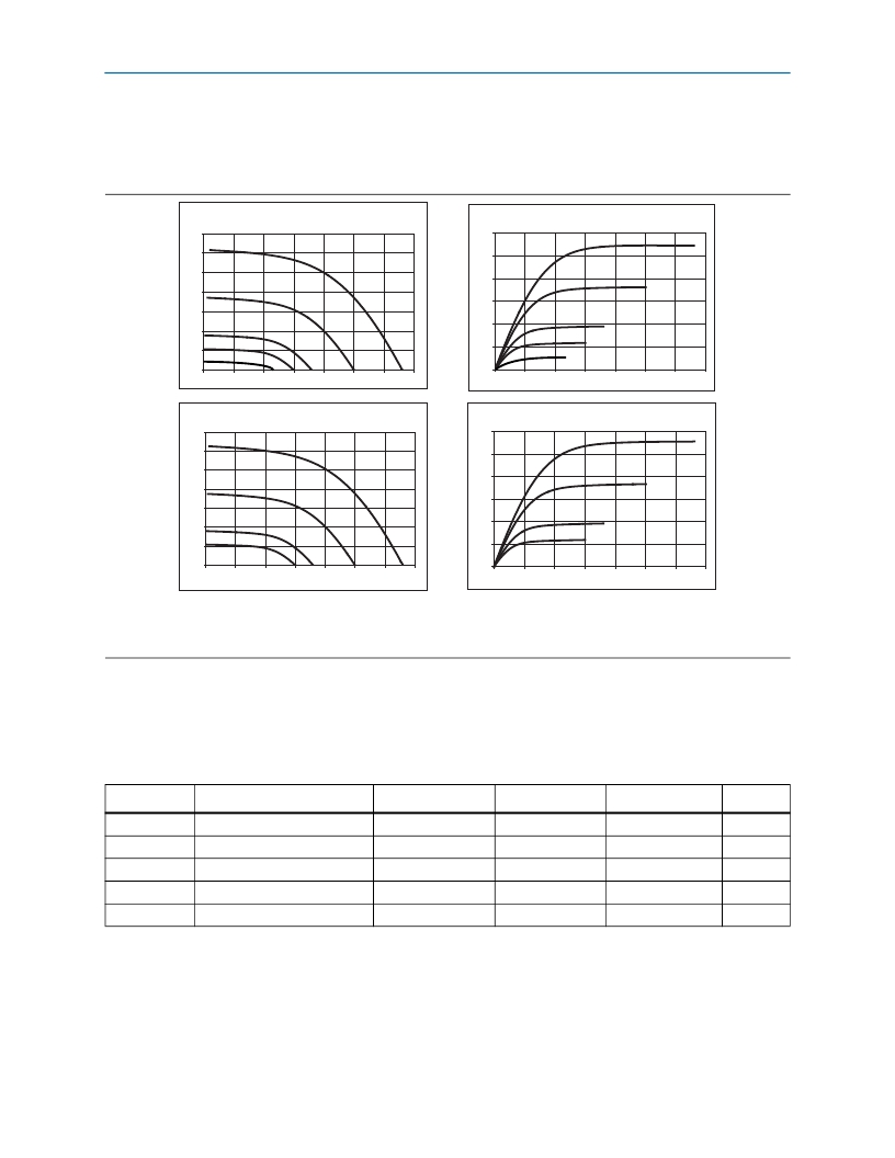
MAX V Output Drive I OH Characteristics
(Maximum Drive Strength)
MAX V Output Drive I OL Characteristics
(Maximum Drive Strength)
70
60
50
3.3-V VCCIO
60
50
3.3-V VCCIO
40
2.5-V VCCIO
40
2.5-V VCCIO
30
30
20
1.8-V VCCIO
20
1.8-V VCCIO
1.5-V VCCIO
10
0
1.5-V VCCIO
1.2-V VCCIO (2)
10
0
1.2-V VCCIO (2)
0.0
0.5
1.0
1.5
2.0
2.5
3.0
3.5
0.0
0.5
1.0
1.5
2.0
2.5
3.0
3.5
Voltage (V)
MAX V Output Drive I OH Characteristics
(Minimum Drive Strength)
Voltage (V)
MAX V Output Drive I OL Characteristics
(Minimum Drive Strength)
35
30
3.3-V VCCIO
30
25
3.3-V VCCIO
25
20
2.5-V VCCIO
20
2.5-V VCCIO
15
15
10
5
0
1.8-V VCCIO
1.5-V VCCIO
10
5
0
1.8-V VCCIO
1.5-V VCCIO
0.0
0.5
1.0
1.5
2.0
2.5
3.0
3.5
0.0
0.5
1.0
1.5
2.0
2.5
3.0
3.5
Voltage (V)
Voltage (V)
(1) The DC output current per pin is subject to the absolute maximum rating of Table 3–1 on page 3–1 .
(2) 1.2-V V CCIO is only applicable to the maximum drive strength.
I/O Standard Specifications
MAX V device family.
Table 3–5. 3.3-V LVTTL Specifications for MAX V Devices
Symbol
V CCIO
V IH
V IL
V OH
V OL
Parameter
I/O supply voltage
High-level input voltage
Low-level input voltage
High-level output voltage
Low-level output voltage
Conditions
—
—
—
IOH = –4 mA (1)
IOL = 4 mA (1)
Minimum
3.0
1.7
–0.5
2.4
—
Maximum
3.6
4.0
0.8
—
0.45
Unit
V
V
V
V
V
(1) This specification is supported across all the programmable drive strength settings available for this I/O standard, as shown in the
May 2011
Altera Corporation
发布紧急采购,3分钟左右您将得到回复。
相关PDF资料
DK-DEV-5SGXEA7N
KIT DEV STRATIX V FPGA 5SGXEA7
DK-DSP-2S180N
DSP PRO KIT W/SII EP2S180N
DK-DSP-3C120N
KIT DEV DSP CYCLONE III EDITION
DK-K7-CONN-CES-G
KINTEX-7 FPGA CONNECTIVITY KIT
DK-K7-EMBD-CES-G-J
KINTEX-7 FPGA EMBEDDED KIT JAPAN
DK-MAXII-1270N
KIT DEV MAXII W/EPM 1270N
DK-N2EVAL-3C25N
KIT DEV NIOS II CYCLONE III ED.
DK-NIOS-2C35N
NIOS II KIT W/CYCLONE II EP2C35N
相关代理商/技术参数
DK-DEV-5SGSMD5N
功能描述:可编程逻辑 IC 开发工具 FPGA Development Kit For 5SGSMD5K2
RoHS:否 制造商:Altera Corporation 产品:Development Kits 类型:FPGA 工具用于评估:5CEFA7F3 接口类型: 工作电源电压:
DK-DEV-5SGSMD5N/P
制造商:Altera Corporation 功能描述:DSP DEVELOPMENT KIT,STRATIX V
DK-DEV-5SGXEA7/ES
功能描述:可编程逻辑 IC 开发工具 FPGA Development Kit For 5SGXEA7 ES
RoHS:否 制造商:Altera Corporation 产品:Development Kits 类型:FPGA 工具用于评估:5CEFA7F3 接口类型: 工作电源电压:
DK-DEV-5SGXEA7N
功能描述:可编程逻辑 IC 开发工具 FPGA Development Kit For 5SGXEA7K2F40C2N
RoHS:否 制造商:Altera Corporation 产品:Development Kits 类型:FPGA 工具用于评估:5CEFA7F3 接口类型: 工作电源电压:
DK-DSP-2C70N
功能描述:DSP KIT W/CYCLONE II EPS2C70N RoHS:是 类别:编程器,开发系统 >> 通用嵌入式开发板和套件(MCU、DSP、FPGA、CPLD等) 系列:Cyclone® II 产品培训模块:Blackfin® Processor Core Architecture Overview
Blackfin® Device Drivers
Blackfin® Optimizations for Performance and Power Consumption
Blackfin® System Services 特色产品:Blackfin? BF50x Series Processors 标准包装:1 系列:Blackfin® 类型:DSP 适用于相关产品:ADSP-BF548 所含物品:板,软件,4x4 键盘,光学拨轮,QVGA 触摸屏 LCD 和 40G 硬盘 配用:ADZS-BFBLUET-EZEXT-ND - EZ-EXTENDER DAUGHTERBOARDADZS-BFLLCD-EZEXT-ND - BOARD EXT LANDSCAP LCD INTERFACE 相关产品:ADSP-BF542BBCZ-4A-ND - IC DSP 16BIT 400MHZ 400CSBGAADSP-BF544MBBCZ-5M-ND - IC DSP 16BIT 533MHZ MDDR 400CBGAADSP-BF542MBBCZ-5M-ND - IC DSP 16BIT 533MHZ MDDR 400CBGAADSP-BF542KBCZ-6A-ND - IC DSP 16BIT 600MHZ 400CSBGAADSP-BF547MBBCZ-5M-ND - IC DSP 16BIT 533MHZ MDDR 400CBGAADSP-BF548BBCZ-5A-ND - IC DSP 16BIT 533MHZ 400CSBGAADSP-BF547BBCZ-5A-ND - IC DSP 16BIT 533MHZ 400CSBGAADSP-BF544BBCZ-5A-ND - IC DSP 16BIT 533MHZ 400CSBGAADSP-BF542BBCZ-5A-ND - IC DSP 16BIT 533MHZ 400CSBGA
DK-DSP-2S180N
功能描述:DSP PRO KIT W/SII EP2S180N RoHS:是 类别:编程器,开发系统 >> 通用嵌入式开发板和套件(MCU、DSP、FPGA、CPLD等) 系列:Stratix® II 产品培训模块:Blackfin® Processor Core Architecture Overview
Blackfin® Device Drivers
Blackfin® Optimizations for Performance and Power Consumption
Blackfin® System Services 特色产品:Blackfin? BF50x Series Processors 标准包装:1 系列:Blackfin® 类型:DSP 适用于相关产品:ADSP-BF548 所含物品:板,软件,4x4 键盘,光学拨轮,QVGA 触摸屏 LCD 和 40G 硬盘 配用:ADZS-BFBLUET-EZEXT-ND - EZ-EXTENDER DAUGHTERBOARDADZS-BFLLCD-EZEXT-ND - BOARD EXT LANDSCAP LCD INTERFACE 相关产品:ADSP-BF542BBCZ-4A-ND - IC DSP 16BIT 400MHZ 400CSBGAADSP-BF544MBBCZ-5M-ND - IC DSP 16BIT 533MHZ MDDR 400CBGAADSP-BF542MBBCZ-5M-ND - IC DSP 16BIT 533MHZ MDDR 400CBGAADSP-BF542KBCZ-6A-ND - IC DSP 16BIT 600MHZ 400CSBGAADSP-BF547MBBCZ-5M-ND - IC DSP 16BIT 533MHZ MDDR 400CBGAADSP-BF548BBCZ-5A-ND - IC DSP 16BIT 533MHZ 400CSBGAADSP-BF547BBCZ-5A-ND - IC DSP 16BIT 533MHZ 400CSBGAADSP-BF544BBCZ-5A-ND - IC DSP 16BIT 533MHZ 400CSBGAADSP-BF542BBCZ-5A-ND - IC DSP 16BIT 533MHZ 400CSBGA
DK-DSP-2S60N
功能描述:DSP KIT W/STRATIX II EP2S60N RoHS:是 类别:编程器,开发系统 >> 通用嵌入式开发板和套件(MCU、DSP、FPGA、CPLD等) 系列:Stratix® II 产品培训模块:Blackfin® Processor Core Architecture Overview
Blackfin® Device Drivers
Blackfin® Optimizations for Performance and Power Consumption
Blackfin® System Services 特色产品:Blackfin? BF50x Series Processors 标准包装:1 系列:Blackfin® 类型:DSP 适用于相关产品:ADSP-BF548 所含物品:板,软件,4x4 键盘,光学拨轮,QVGA 触摸屏 LCD 和 40G 硬盘 配用:ADZS-BFBLUET-EZEXT-ND - EZ-EXTENDER DAUGHTERBOARDADZS-BFLLCD-EZEXT-ND - BOARD EXT LANDSCAP LCD INTERFACE 相关产品:ADSP-BF542BBCZ-4A-ND - IC DSP 16BIT 400MHZ 400CSBGAADSP-BF544MBBCZ-5M-ND - IC DSP 16BIT 533MHZ MDDR 400CBGAADSP-BF542MBBCZ-5M-ND - IC DSP 16BIT 533MHZ MDDR 400CBGAADSP-BF542KBCZ-6A-ND - IC DSP 16BIT 600MHZ 400CSBGAADSP-BF547MBBCZ-5M-ND - IC DSP 16BIT 533MHZ MDDR 400CBGAADSP-BF548BBCZ-5A-ND - IC DSP 16BIT 533MHZ 400CSBGAADSP-BF547BBCZ-5A-ND - IC DSP 16BIT 533MHZ 400CSBGAADSP-BF544BBCZ-5A-ND - IC DSP 16BIT 533MHZ 400CSBGAADSP-BF542BBCZ-5A-ND - IC DSP 16BIT 533MHZ 400CSBGA
DK-DSP-3C120N
功能描述:可编程逻辑 IC 开发工具 FPGA Development Kit For EP3C120F780
RoHS:否 制造商:Altera Corporation 产品:Development Kits 类型:FPGA 工具用于评估:5CEFA7F3 接口类型: 工作电源电压:
